GPS frequency counter
As an exercise in FPGA design, I built a frequency counter using a cheap GPS module for a timing reference.
It turns out that the extremely popular ublox NEO-6 series of GPS modules, which can be purchased on eBay for around ~10$, is capable of producing a relatively accurate pulse-per-second output.
The same manufacturer also sells special timing versions of their modules with mildly improved parameters, but these were much harder to get in low quantities at the time I was ordering the components (there are some available on ebay currently).
Note: The NEO‑6 have since been discontinued and was replaced by the NEO‑M8 series. These modules also have the PPS output with similar parameters.

Using the GPS system like this enables us to “borrow” an ultra-expensive atomic clock (in orbit).
Measurement method
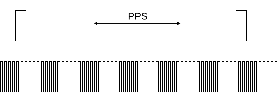
There are multiple measurement methods for measuring oscillators. As my reference clock is generally several orders of magnitude slower than the measured oscillator, the only reasonable approach is to count the cycles between PPS pulses.
(excuse the crudity of the measurement, the probe isn’t attached properly and the scope is hitting its bandwidth limitations)
Error analysis
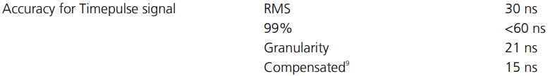
Overall, we have two problems — first being our individual PPS pulses might not be precisely one second (this is mostly caused by our receiver, the satellites are “exact enough”). Second is the quantization error caused by the measurement method — we have no way of getting the “fractional” value. In other words, there is no way of distinguishing if the timing pulse arrived at, for example, .1 or at .8 of a cycle.
Let’s do some mildly naive interval error analysis:
- - Is the base PPS period (1 second)
- - Is our PPS period interval (1 second ±60 ns)
- - is the real frequency of our oscillator
- - our estimate of
- - relative error of with respect to
Even for and , this works out to just the ±0.5 rouding error ( is really small compared to our measurement interval). Poking at symbols for a bit leads to:
As changing the measured frequency isn’t usually practical, we are left with manipulating our integration time to get to the desired precision. For instance, given a 10 MHz oscillator, this gets us to ±0.1 ppm at 1 second, 0.01 ppm at 10 seconds…
Unfortunately I don’t have any good frequency reference to figure out if these error calculations actually estimate the measured value properly.
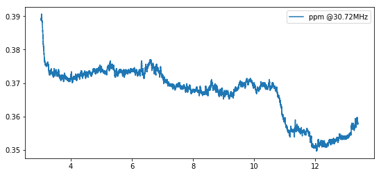
The plot below shows a ~12-hour measurement (100 seconds of sliding average) of the TCXO inside my LimeSDR. Given the parameters of the oscillator, the values seem pretty sensible.
Hardware
FPGA
I went with a small MAX 10 series FPGA. These FPGAs contain integrated flash memory for storing the configuration and also are capable of operating from just a single 3.3V power supply rail. This brings the amount of additional circuitry required to the level of an average microcontroller.
Beware of the “compact features” variants, as they don’t support SRAM initialization nor custom user flash partition. This makes loading firmware to a softcore pretty inconvenient.
Unfortunately the only non-BGA version available (I don’t have very good track record of manual BGA soldering) is the humongous 144-pin QFP. This at least allows me to use just a two layer board though.
Board
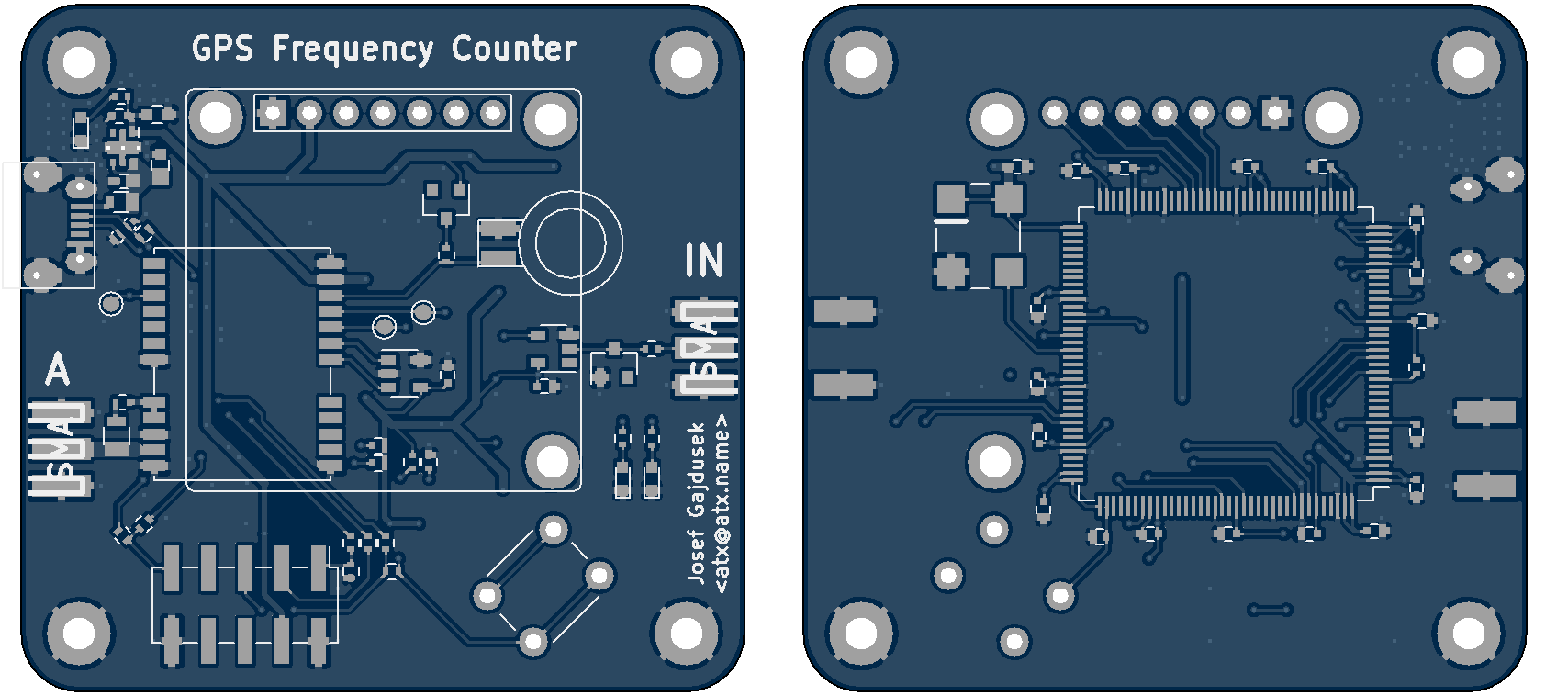
There is nothing really special on the board — it’s essentially just the FPGA, the GPS module and the OLED with some supporting circuitry.
As using an active antenna usually helps GPS reception considerably, the board has a bias-T providing 3.3 V to the antenna connector.
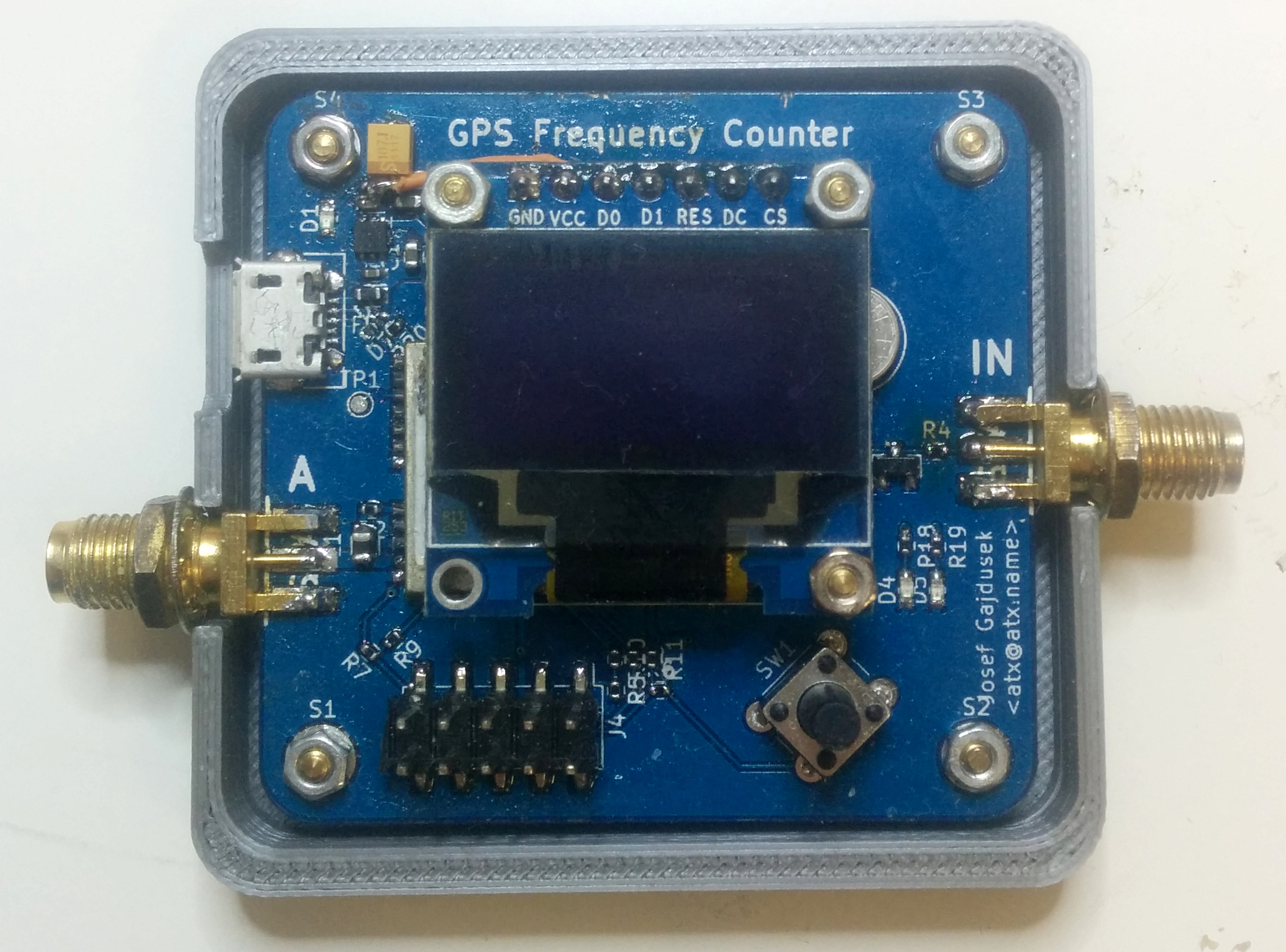
Bill of materials
(Only the interesting parts anyway)
| Name | Description |
| 10M08SCE144C8G | MAX10 FPGA in QFP |
| Ublox NEO-6M | GPS module with PPS output |
| OLED module | SSD1306-based OLED module with SPI interface |
| 24AA32AT | EEPROM for the GPS module |
| LP5912 | 3.3V linear regulator |
| MS621FE | SMD coin cell battery for the GPS module |
| SN74LV1T34DBVR | Single channel CMOS buffer |
Firmware
I wrote the FPGA gateware in Chisel with some occasional Verilog plumbing. In total, the design eats up just around ~40% of the available logic elements of the FPGA. Almost all of the memory blocks are consumed, but I haven’t performed even the most obvious optimization (such as running the code directly from flash or at least keeping the graphic data there).
The design centers around the PicoRV32 RISC-V softcore with a bunch of custom peripherals. The processor does everything from talking with the GPS module over UART to drawing the UI on the OLED screen to handling the higher levels of the USB stack.
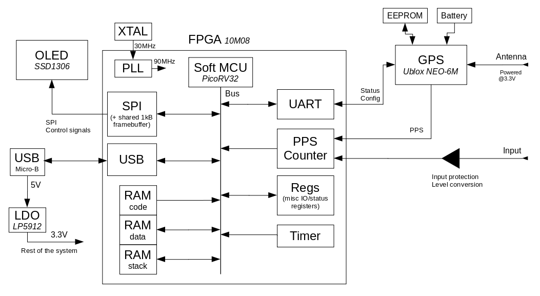
USB Stack
Inspired by a talk at 33C3, I decided to implement a primitive USB stack. The onboard USB connector was primarily intended for power delivery, but connecting the data pair just-in-case to the FPGA was a no brainer.

The stack runs at low-speed (1.5Mb/s) and can do only a somewhat limited subset of the usual USB capabilities — only control transfers are supported. Altough this is not good enough to implement most of the “standard” USB devices (like emulated serial port), it is sufficient to read out the counter value and perform “long-term” measurements.
Source
The project is released under the MIT license. All of the source code and PCB drawings can be found on my GitHub.